Routing the Front Panel PCB (optional)
Overview
By default, the front panel PCB is generated automatically but involves some more soldering than really needed: We’ve put pads for the back board pins you use, and you need to solder each pad of the headers to each pad of the destination component. For most components, there is just one wire to solder on each side, so you might have approximately as many wires to solder as you have controls on your module. While this is not so long to assemble, but still makes more soldering, and so lengthen the whole assembly time.
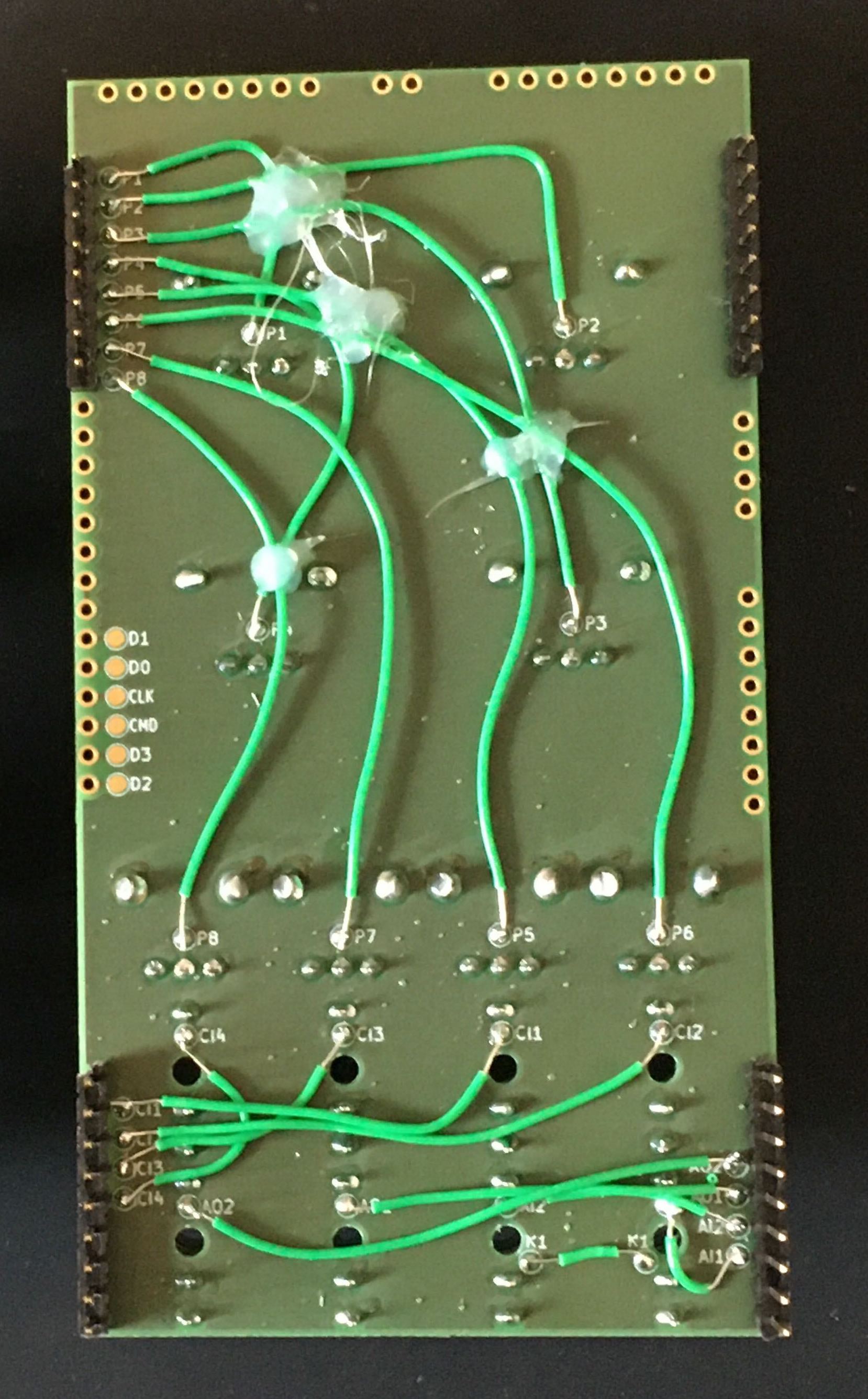
The picture below shows a module assembled with wires only, so you have an idea on how much work is involved. This module has 8 pots, 4 CVs, 2 audio inputs and 2 audio outputs:
So, Eurorack-blocks automate everything for us, why doesn’t it also route this automatically for us? Good question! The problem lies in that it is not possible to fully automate auto-routing (the process of connecting those pads on the PCB itself) with Kicad 5 and 6 for various technical reasons. We are working on it, but in the meantime, you can do manually what is not possible to automate, and this is quite straightforward when you get used to it.
For this, you need to know Kicad a bit. Not much, but still the interface is quite different to what you can be used to. But if you want to try win some time, just follow along the instructions below.
And if you are not comfortable with this, no problem! Just order your PCB in the next chapter, and you will just have a bit more soldering to do when assembling your front panel PCB.
Requirements
Setting up Manual Routing
First, add an option to your Erbui file to instruct that you will route the PCB manually.
// Kick.erbui

module Kick {
   route manual
   ...
}
What it does is to instruct to not generate the gerber files, and not generate pads for the headers, to have more space to route.
eurorack-block/$ cd samples/kick/
eurorack-block/samples/kick/$ erbb build hardware
eurorack-block/samples/kick/$ ls -l artifacts/hardware/
total 968
-rw-r--r--   1 raf  staff    1198 Feb 17 09:07 Kick.bom.csv
-rw-r--r--   1 raf  staff   17781 Feb 17 09:07 Kick.dxf
-rw-r--r--   1 raf  staff  113944 Feb 17 09:07 Kick.gerber.zip
-rw-r--r--   1 raf  staff  338644 Feb 17 09:07 Kick.kicad_pcb
-rw-r--r--   1 raf  staff   15965 Feb 17 09:07 Kick.pdf
drwxr-xr-x  12 raf  staff     384 Feb 17 09:07 gerber
Now open the Kick.kicad_pcb file, which should look like this:
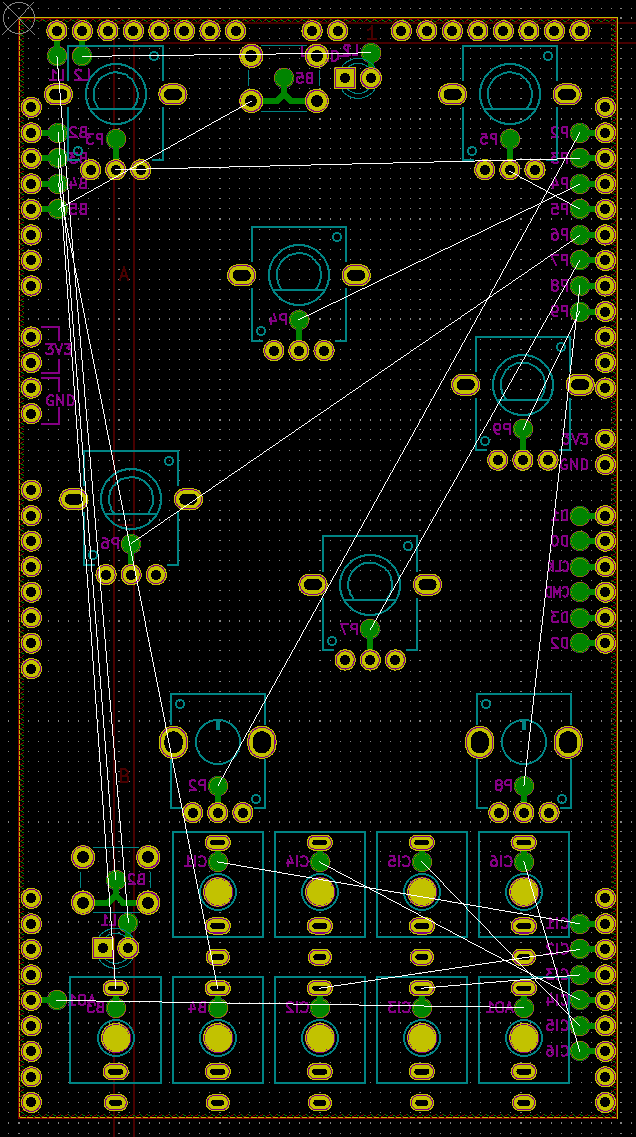
The white lines, called the ratsnest, indicates you what needs to be routed to what. From there you could route the PCB traces entirely manually, but we can also use an autorouteur for that. It might not be the best PCB layout ever, but that will be good enough for a prototype.
Autorouting
Follow the instructions on this Freerouting page, it also contains a video to show you how it is done, step by step.
Generating Gerber Files
Now that we have our kicad_pcb file properly routed, we can generate the final
Gerber files that we will need to use in the next chapter.
For this run:
eurorack-block/samples/kick/$ erbb build hardware --only-gerber
That’s done! Now you are good to go and order everything before you assemble your module.