Soldering the Back Board
Overview
Every Eurorack-blocks project comes with a back board, which mediates between the Daisy Patch Submodule and your custom front panel. In a nutshell, this back board extends the functionalities of the Daisy Patch Submodule using components that are more or less some sort of multiplexers or demultiplexers, as well as forwarding feature pins accordingly, for example either keeping the SD signals on the back board, or making them accessible to the front panel, or a combination of boths (using jumpers).
Back boards are made for mass-production, and given their density, SMD components usage is a constraint. As such, you need to be either being able to solder them, or have a PCB Assembly (PCBA) service do it for you, or buy it from us (coming soon).
Generating Manufacturing Files
You first need to generate everything you need.
Let’s take the 12HP board kivu12
as an example, but every boards provides the same features.
First go to the board folder, and call build.py to generate everything needed
for manufacturing:
eurorack-block/$ cd boards/kivu12/
eurorack-block/boards/kivu12/$ ./build.py
eurorack-block/boards/kivu12/$ ls -l artifacts/
total 496
drwxr-xr-x  12 raf  staff     384 May 11  2021 gerber
-rw-r--r--   1 raf  staff  157640 Feb 10 01:58 kivu12-gerber.zip
-rw-r--r--@  1 raf  staff    5340 Feb 10 01:58 kivu12.bom.digikey.csv
-rw-r--r--@  1 raf  staff    9020 Feb 10 01:58 kivu12.bom.csv
-rw-r--r--   1 raf  staff    4048 Feb 10 01:58 kivu12.pickplace.txt
kivu12-gerber.ziprepresents the PCB informations for the manufacturer. You typically upload this file to your PCB manufacturer,kivu12.bom.digikey.csvis the Bill of Materials (BOM) of the components you need to buy, in a format compatible with the Digikey global supplier,kivu12.bom.csvis the same BOM but in a generic format suitable for PCBA services,kivu12.pickplace.txtis an instruction file for a Pick & Place machine, you only need this when you are doing PCBA, that is asking your board manufacturer to also assemble the PCB with the SMD components, if they provide this service.
Ordering the PCB
Go to your favorite PCB manufacturer, here Beta-layout in Europe,
and use the kivu12-gerber.zip file
(usually using drag & drop), to upload the PCB gerber files.
Depending on your PCB manufacturer, this shoud look like this:
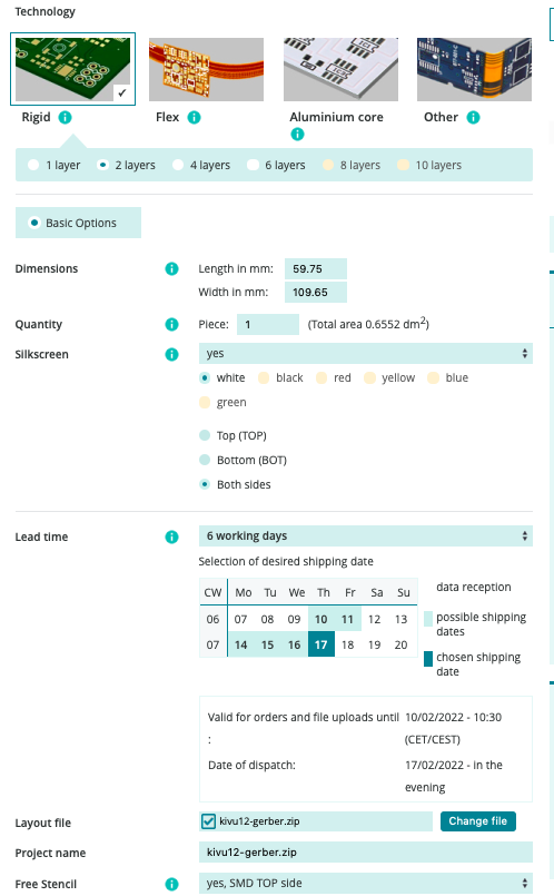
Make sure that:
You are ordering a 2-layer board,
The height is around (but very closely to) 109.65mm,
The silkscreen is printed on both sides,
You get a SMD stencil for the top side if you are doing hot-air soldering.
Then the amount of boards is up to you. Usually getting at least 5 boards is a good idea, so maybe first talk with friends to know who would want some!
The PCB manufacturer shown upper is producing the PCB in Germany. If you are living in Europe, this is very handy because you don’t need to deal with long delivery times and customs processes. However that also comes at a higher price!
If you want to save on that, you can produce abroad, for really cheaper PCB, but at the expense of a longer delivery time. Should you choose this option and the PCB manufacturer offers a DDP option for delivery, go for it! DDP means “Delivery Duty Paid (legally much more as part of incoterms) and saves you a lot of time potentially when dealing with customs, and the import taxes are pre-paid by the transporter, saving yet more time when receiving the package.
Ordering the BOM
The BOM is made to be compatible with the automatic BOM importer for the Digikey global supplier. Go to the Digikey website and select your country. Create a new account if you don’t already have one.
Then go to their list manager
and click the Upload a List button. Locate the BOM file and upload it.
For the kivu12 board this is the kivu12.bom.digikey.csv file on your disk
in the eurorack-blocks/boards/kivu12/artifacts folder.
Once imported, this should look like that:
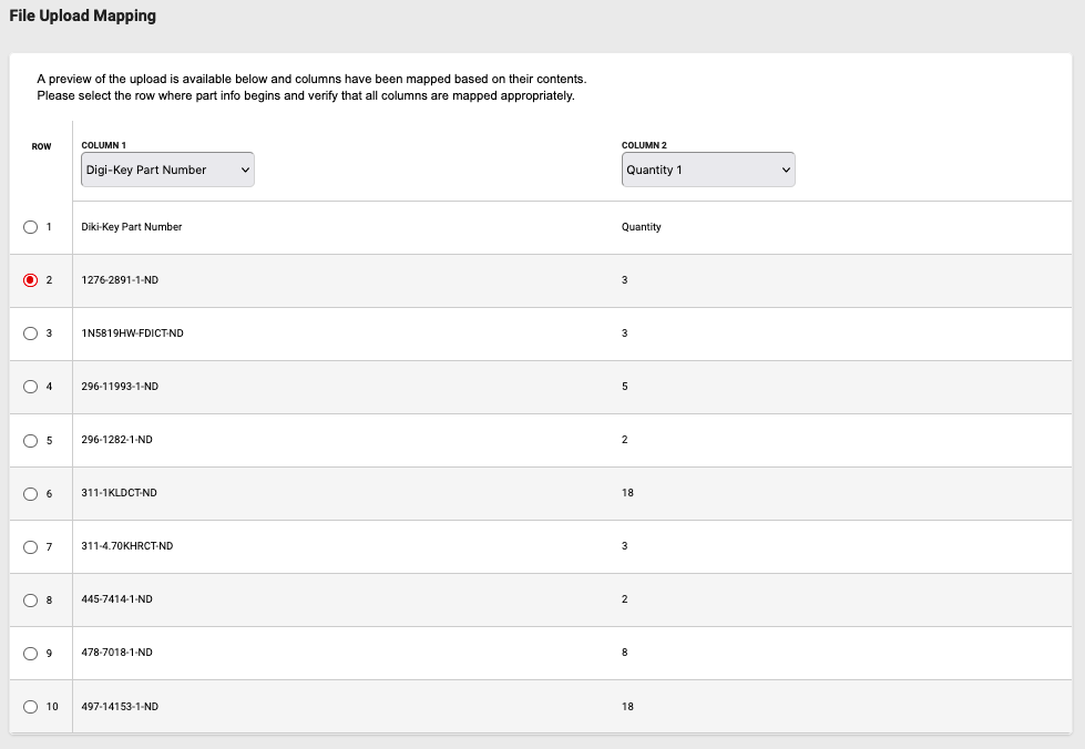
Make sure that the second row is selected in the radio buttons on the left side, which indicates the first line to take into account in the spreadsheet. Then click on the Continue to List Preferences button, and finalize the upload. You then get on a page like that:
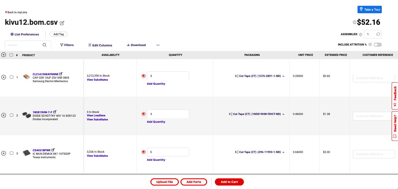
Make sure to select your number of assemblies (on the top right corner), that is the number of times you are going to build the board. Normally this number should follow the same number of PCBs you ordered. For example, if you ordered 5 PCBs, you should order 5 assemblies.
Finally, you can add to the cart, and review the options they give you such as:
Order more parts for a specific components to get to a better price because of the price break (anyway it is always a good idea to have at least 10% components more than needed),
Replace components that are not available by a direct remplacement.
Go to the payment page, and if you are leaving outside of the US, prefer a delivery that has the DDP option (Delivery Duty Paid), as this speeds up delivery considerably faster.
That’s it! Now you will probably receive your BOM very quickly, and will wait for your PCBs a bit longer. When you receive everything, it is finally time to assemble everything!
Assembling the Board
Gather all your components to make sure you are not going to miss some or search for some later. Put on your lab coat, gather a pair of gloves and safety glasses, get your anti-static grounding wrist strap at hand, and ensure proper ventilation.
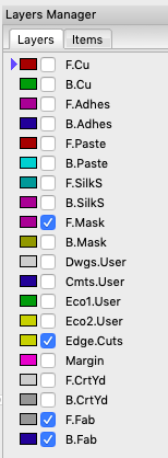
Take also your computer and open the board .kicad_pcb file. In the right
column in the Layers Manager, hide all layers except the F.Mask, Edge.cuts, F.Fab
and B.Fab layer. That should look like this:
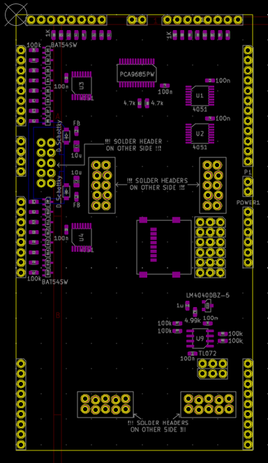
This schematic gives you a nice plan of what components to place where. You are now ready to solder your boards!