Checking for Mistakes
Overview
The front panel consists of a PCB on which your components such as pots, buttons and LEDs will be soldered too. Those components have what is called a “footprint” which defines, for our current interest, some copper-plated holes to which you will solder your components.
In the software world, we can place our widgets wherever we see fit, and as long as it looks good on screen and the user experience is satisfactory, we can go on with it. It’s a bit different in the hardware world, for two main reasons:
We need to ensure there is enough space between the panel elements, so that you can put your fingers between them. Typically, if you put two pot knobs too close to each others, your users might have a problem to rotate one knob without mistakenly rotating the other one,
We need to ensure that we don’t make electrical shorts on the boards, when 2 elements are too close to each others, or all sorts of similar problems, like having two drill holes too close to each others, etc.
This chapter addresses the latter point.
Generating Manufacturing Files
You first need to generate everything you need.
Let’s take the Kick module
as an example, but you can do the following with any other modules.
First go to the module folder, and call erbb build hardware to generate everything needed
for manufacturing:
eurorack-block/$ cd samples/kick/
eurorack-block/samples/kick/$ erbb build hardware
eurorack-block/samples/kick/$ ls -l artifacts/hardware/
total 968
-rw-r--r--   1 raf  staff    1198 Feb 17 09:07 Kick.bom.csv
-rw-r--r--   1 raf  staff   17781 Feb 17 09:07 Kick.dxf
-rw-r--r--   1 raf  staff  113944 Feb 17 09:07 Kick.gerber.zip
-rw-r--r--   1 raf  staff  338644 Feb 17 09:07 Kick.kicad_pcb
-rw-r--r--   1 raf  staff   15965 Feb 17 09:07 Kick.pdf
drwxr-xr-x  12 raf  staff     384 Feb 17 09:07 gerber
The Kick.kicad_pcb is the Kicad PCB file that was automatically generated from your
Erbui definition files.
Using the Design Rule Checker
You may place components on the board in a way where they collide with each others. When using the GUI editor (coming soon), those checks are automatically done for you. However if you make late changes to your design, and as a general guideline, you will want to make sure that your design can be properly produced.
For this we use what is called a Design Rule Checker (DRC), and Kicad contains one.
Open your Kick.kicad_pcb file and locate the ladybird button on top of the interface:
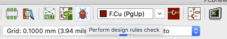
Then click it, and run the DRC. It will show red arrows where the DRC found problems you need to correct. Below is shown the original design of the Kick module and you can see it had problems! So that’s always a good idea to double-check.
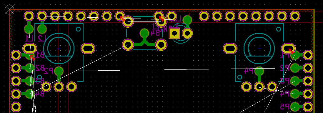
How can we solve those? Usually there are 2 main strategies. Using the screenshot upper as an example:
You can move the part so that it doesn’t collide. In the original Kick, we had to do that for the middle-top button, so we decided to move down a bit, in the Erbui file, both the button and its associated LED,
You can exclude the use of some pins. In the original Kick, we see that
B1andP1are colliding with the top pots, so if we don’t want to move those 2 pots, we can just explicitly exclude those 2 pins in our Erbui file.
Typically here, excluding pins B1 and P1 in Erbui would be done this way:
   module Kick {
   board kivu12
   material aluminum
   header { label "KICK" }

   exclude pins B1, P1

   // Trigger ----------------------------------------------------------------
After we excluded pins moved components and re-run erbb build hardware,
the DRC checker is happy, and we can proceed with autorouting or ordering the PCB.
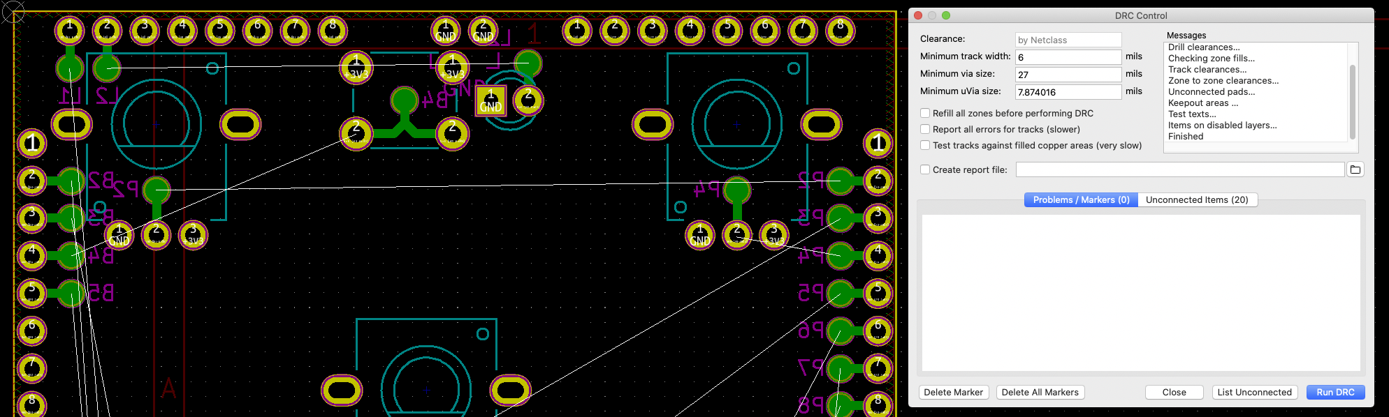
You can see that we have a lot of unconnected elements, but this is normal. You can either solder pads manually, or use autorouting in the next chapter. If you use autorouting, the number of unconnected items should be 0.